SEMICONDUCTOR PHYSICS
SEMICONDUCTOR:
It has electrical conductivity that lies between conductor and
insulator.
e.g., Silicon,
Germanium
TYPES
INTRINSIC SEMICONDUCTOR – PURE FORM
EXTRINSIC SEMICONDUCTOR – IMPURE FORM
INTRINSIC SEMICONDUCTOR:
It is a crystalline structure and atoms are arranged in uniform
periodic pattern.
CONDUCTIVITY OF INTRINSIC
SEMICONDUCTOR:


The conductivity is initiated by giving some external voltage
greater than forbidden energy gap.
When the external voltage applied (or at room temperature), a bond
will be broken and an electron is freed from atom and it constitute a current.
And the dislodging electron leaves positive charge in that place
called as hole.
This forms electron-hole pair.
The hole has equal magnitude as that of electron.
GENERATION AND RECOMBINATION OF
ELECTRONS & HOLES:
How electrons constitute electric
current??????????????


The external energy required for silicon is 1.1eV and for
germanium is 0.72eV.
When the external energy applied, the bond broke and electron
moves to conduction band.
The dislodging electron produces hole in that place.
Conduction of electron is also done by increase in temperature.
As the temperature is further increased more and more electrons
are produced also the electron-hole pair produces.
Hence electrons in the conduction band keep on increasing simultaneously
holes also increasing in the valence band.
This gives a way for conduction of intrinsic semiconductor by
electrons.
How holes constitute electric
current???????????????

The current is produced by means of flow of charge.
Electron current produces by the movement of electrons from
valence band to conduction band.
Similarly, hole current produces by the recombination of holes and
electrons inside the crystal.
When an electron moves to conduction band hole (I) produced in
that place.
As the temperature further increases the electron in the vicinity
dislodge and produce hole(II).
Now the hole at the 1st location recombines with the new electron
produced at 2nd location.
This process continues and the movement of hole takes place from
one place to another.
So this constitutes hole current.
EXTRINSIC SEMICONDUCTOR:
The process of adding impurity to a pure semiconductor is called extrinsic
semiconductor.
The process of adding impurities is called doping. The added
impurity is called dopant.
Two types:
N-type semiconductor
P-type semiconductor
N-Type semiconductor:
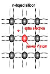
The n-type material is formed by doping pentavalent impurity atoms
like P, As, Sb, etc., at a low rate with silicon/germanium.
The process of adding pentavalent impurities to a semiconductor is
called as N-Type semiconductor.
When it is added and forms covalent bond one electron doesn’t form
any bond (since contains 5 valence electrons).
That electron remains as free electrons and constitute current.
CONDUCTION:

The pentavalent impurities form an additional level called donor level (near edge of conduction band).
At absolute temperature, valence band is filled, conduction band
is empty and donor level is filled.
But at room temp, the valence electrons gain some energy and moves
to conduction band and constitute current.
At the same time the electrons in the donor level is also moved to
conduction band.
So the combination of electrons from valence band and donor levels
gives more current.
As the constitution of current is by means of electrons this
material is called n-type material.
NOTE: Even though n-type produces the
large number of electrons the atom is still electrically neutral.
P-Type semiconductor:

The p-type semiconductor is formed by adding trivalent impurity
such as boron, gallium, indium, etc.,
The process of adding trivalent impurities to a semiconductor is
known as P-Type semiconductor.
When it is added and forms covalent bond there will be an
insufficient electron and holes produced in that place (3 valence electrons).
That hole constitute current called hole current.
CONDUCTION:

The trivalent impurity produces additional level called acceptor
level near the valence band.
At zero temperature valence band is filled by holes, acceptor
level is empty and conduction band is also empty ( in terms of holes).
But at room temperature, minimum electrons in valence band moves
to conduction band also to acceptor level.
So the holes increased in valence band thus constitute hole
current.
Thus the increase in holes concentration constitutes more hole
current.
For this reason this type is called p-type semiconductor.
No comments:
Post a Comment